
The 6th R.O.C. ( Taiwan )Presidential Innovation Award Report_Individual Category_National Tsinghua University Burn J. Lin, Distinguished Research Chair Professor



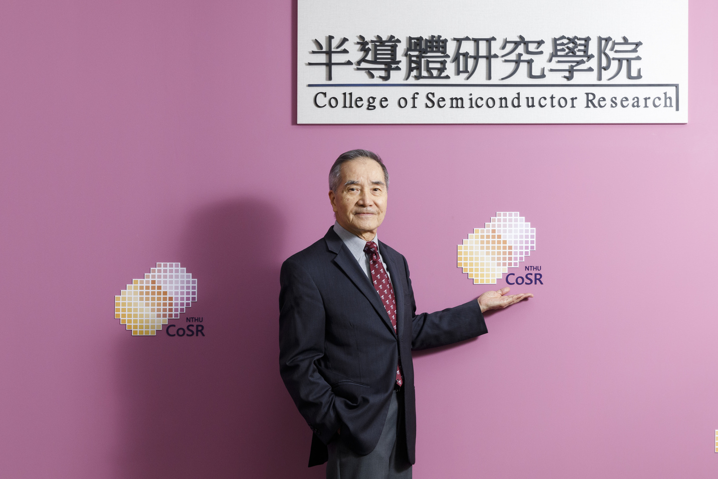
Burn J. Lin, Distinguished Research Chair Professor
National Tsinghua University
Individual Category
Leaping Six Generations: The Odyssey of an Immersion Lithography Expert in Mass Production
Tracing the history of semiconductor technology, Academician Burn J. Lin, a foremost scientist in optical lithography, made a pivotal contribution by introducing the concept of immersion lithography using water as the medium at the 193 nm vacuum wavelength. He successfully convinced the industry to adopt this as a mainstream technology. This groundbreaking process, evolving from theoretical invention to mass production on the production line, positioned Taiwan to set industry standards for the first time. It enabled the country to leapfrog six technological generations and emerge as a global leader. Holding numerous prestigious titles, Burn remains committed to advancing semiconductor education in his later years, spearheading a newly established college dedicated to nurturing domestic semiconductor talents.
When I began working with projection lithography, the minimum linewidth was 2000 nm. Now, it has been reduced to 5 nm. With each generation shrinking by about 70%, we have progressed through sixteen generations. God orchestrated my journey to IBM, providing me with the prime opportunity to contribute to the advancement of semiconductor technology. Later, the fortuitous chance to join TSMC and apply my research on a leading mass production platform was a remarkable turn of events." ── Burn J. Lin, "Put Your Mind on Your Life, Work, and Family" , 2018
In 1942, Burn J. Lin, a second-generation overseas Chinese, was born in Cholon, near Saigon, (now Ho Chi Minh City) Vietnam. His father, William Lin, an educator, founded Vietnam's first English school, William Lin Middle School. At 16, he came to Taiwan by himself, with a camera and blessings from his elders, and enrolled at Hsinchu Senior High School. After earning his degree in Electrical Engineering from National Taiwan University, he went on to obtain a doctoral degree from Ohio State University in the United States.
In his book "Put Your Mind on Your Life, Work, and Family", Burn recounts how his doctoral dissertation advisor, Stuart A. Collins, introduced holography to Ohio State University. "After learning about holography, I wanted to focus on nothing else. Because of my passion for photography, the ability to accurately preserve three-dimensional images held significant meaning for me. So I became his student, focusing my research and dissertation on holography."
Before completing his Ph.D., he heeded his advisor's recommendation to send job applications to industry members listed in The Journal of the Optical Society of America, as these large optical research institutions were seeking researchers with doctorates. Despite not hearing back from companies like Kodak and Itek that he was keen on, he landed an interview invitation from IBM's Thomas J. Watson Research Center.
"Why would a computer company engage in optical research? How am I of use to them?" He still attended the interview and was scheduled to give a presentation that included advanced equations and experimental data. Two weeks later, he received an offer from IBM.
IBM Ventures into Photolithography: Pioneering Alone in Deep Ultraviolet Light
Burn J. Lin's tenure at IBM marked the start of his journey into the world of optical lithography. At the time, IBM was employing near-field imaging technology for semiconductor chip production and bubble memory disks, which offered ten times higher density than semiconductors. He was involved in developing both technologies, which taught him the processes of using photoresists.
Burn J. Lin's tenure at IBM marked the start of his journey into the world of optical lithography. At the time, IBM was employing near-field imaging technology for semiconductor chip production and bubble memory disks, which offered ten times higher density than semiconductors. He was involved in developing both technologies, which taught him the processes of using photoresists.
Notably, IBM had a large team working on X-ray lithography, similar in scale to today's EUV lithography efforts, while Burn led a much smaller group focused on developing DUV lithography. Despite repeatedly highlighting the reasons why X-rays could not be used for features smaller than 250 nm as well as many other reasons and that the budget for DUV would only be one-tenth of that for X-rays to achieve results surpassing those of competitors, he struggled to secure the necessary funding.
X-ray lithography, similar in scale to today's EUV lithography efforts, while Burn led a much smaller group focused on developing DUV lithography. Despite repeatedly highlighting the reasons why X-rays could not be used for features smaller than 250 nm as well as many other reasons and that the budget for DUV would only be one-tenth of that for X-rays to achieve results surpassing those of competitors, he struggled to secure the necessary funding.
As near-field imaging approached its theoretical limits, Burn shifted to using lens imaging for projection lithography, which became a cornerstone for advancing Moore's law. In this highly challenging and opportunity-rich field filled with skilled professionals, he continued to make significant research and invention contributions. These included uncovering the previously unknown impact of simulated machine vibrations on imaging tolerance in photolithography; developing techniques for optical proximity correction (OPC) generated by increasing resolution, which became essential in semiconductor production; and advancing Moore's Law by six generations through immersion lithography.
Entrepreneur at 50: TSMC Invites His Return to Taiwan
After 16 years at IBM's Watson Research Center, Burn was relocated to Burlington, Vermont, to lead forward-looking research and development at its semiconductor plant. The goal was to develop technology two generations ahead of mass produced products, with a focus on 0.5 and 0.35 micron DRAM. Following the breakthrough in phase shift mask within the photolithography field, Burn was sent to Austin, Texas, by the SEMATECH consortium (Semiconductor Manufacturing Technology) to help advance this technology. This role provided him with increased opportunities to collaborate with photolithography experts from other companies.
Approaching his fiftieth birthday, IBM announced an early retirement package for employees. Initially, he hadn't considered retiring, but colleagues in New York persuaded him to take advantage of the generous retirement plan, warning that terms might worsen in the future. The idea of early retirement started to take shape.
"My position at IBM was very secure, almost like a guaranteed lifelong job. The decision came down to whether to spend an entire lifetime at IBM or venture out and start my own business." Burn's inventions had earned numerous patents for the company. By starting his own business, he could secure patents for his own company and concentrate on what he deemed most important. The downside was the need to rebuild the entire support structure from scratch. After deciding to take the early retirement package and leave his job of 22 years, Burn founded his own company, naming it Linnovation (Lin + Innovation).
In February 2000, nine years after founding his company, Burn unexpectedly received an invitation from then TSMC Vice President Chiang Shang yi to join the company. Initially, Chiang planned to establish two departments: one dedicated to chip photolithography and the other to photomasks. Burnbelieved that the imaging of chips and masks had many synergies and should be developed together-- a very forward-thinking idea.
Later, he was invited to fly to Taiwan in March to meet with a group of senior executives at TSMC. "The interview went smoothly. Some had heard my speeches, others had taken my classes, and a few were former colleagues from IBM. The only person I didn't know beforehand was Vice President Chiang," said Burn.
Burn's excitement stemmed from realizing that his expertise perfectly aligned with the needs of TSMC, a highly successful company. He saw a group of intelligent and capable individuals, with whom he saw the potential to collaborate and achieve great things. However, as a devoted Christian who came to faith at the age of 14, he always sought the Lord's will when making important decisions. This time, the answer to his prayer came rom 1 Corinthians 2:9 in the Bible: "What no eye has seen, what no ear has heard, and what no human mind has conceived—the things God hath prepared for those who love him."
In April of that year, Burn left behind 38 years of life in the US and moved to Hsinchu with his wife.He then led TSMC's Micro Patterning Technology Division (MPTD), which later became Nano Patterning Technology Division (NPTD), for 15 years, during which the team members expanded from 50 to over 700. By the time he retired in 2015, the hotolithography generation had advanced from 130 nm to the brink of mass-producing 7 nm technology, with research and development moving towards 5 nm.
The Perfect Match - Water as a Medium at a 193nm vacuum Wavelength
In his preface to Burn's book, Chiang Shang yi, former co-COO of TSMC, highlighted Burn's most significant contribution to semiconductor technology development: proposing the concept of immersion lithography and successfully convincing the industry to adopt it as a mainstream technology.
In 2002, the industry was poised to replace 193 nm with 157 nm. However, the challenge was producing the perfect lens material that could enable high-fidelity imaging of deep ultraviolet light at 157 nm. At this critical juncture, Burn diverged by proposing a new concept of immersion lithography using water as the medium at the 193-nm dry wavelength.
In Putting Your Mind on Your Life, Work, and Family, Burn elaborates on the innovative journey from invention to mass production. He actually proposed the concept of immersion as early as 1987, but it wasn't until all dry lithography innovations were exhausted, the 45-nm node was at stake, and a research report from MIT Lincoln Laboratory was published on the refractive index of various liquids Burn discovered that using water as a medium for the 193 nm dry wavelength was the optimal solution for semiconductor production.
That study primarily focused on 157nm immersion fluids, but these fluids had low permeability and were oil-based, with some of them even posing a risk of contaminating the chips. Fortunately, the Lincoln Lab people also measured the refractive index of water and found it to be 1.46 at the 193 nm dry wavelength. Due to the lack of transparency, the refractive index of water at 157 nm wavelength could not be measured nor could be used for imaging.
"When I saw the number 1.46, something clicked." Burn's knew that the refractive index of water is around 1.3 at normal wavelengths, so using water as an immersion medium could only improve it by about 30%. Switching to the available shortest wavelength of 193 nm, with a refractive index of 1.46, water could increase the resolution by 46%, avoiding all the challenges associated with 157 nm. This offered higher resolution than the 157 nm, and since water was already widely used in semiconductor production lines, its acceptance was not an issue. It truly was a perfect match.
In September 2002, Burn was invited to speak on immersion lithography at a workshop on 157 nm technology. He pointed out using water at 193 nm could advance technology by one generation beyond the dry process of 157 nm and was easier to develop. It garnered an enthusiastic reception and sparked widespread discussions among everyone during the break.
The ripple effect continued to grow. By February 2004, at the SPIE International Conference on Photolithography, thousands crowded the venue for the 193 nm immersion lithography presentations, overshadowing the 157 nm session which was attended mostly by speakers.
Optical Experts Unite: ASML and TSMC Achieve Successful Mass Production
However, such a landslide proposal hit both supporters and opponents alike, causing quite a stir in the technology communities and even more so among business interests. To persuade experts in the field, Burn spent months traveling to the United States, Europe, and Japan, exchanging ideas with major equipment manufacturers and potential users. Meanwhile, Chiang defended him against backlash from interest groups in Taiwan.
Burn led his team in publishing papers at international conferences, demonstrating the feasibility and advantages of immersion lithography from a theoretical perspective. They also refuted various negative misconceptions and applied for patents early on. Most importantly, it was necessary to persuade manufacturers to supply the machines.
Convincing scanner manufacturers to research, develop, and mass-produce immersion machines was challenging. At that time, the global R&D direction was focused on 157 nm, with investments exceeding US$ 1 billion; one aligner manufacturer claimed to have invested over US$ 700 million.
For this reason, Burn's team traveled to the Netherlands, Germany, the United States, and Japan for technical and business discussions. After over a year of diligent efforts, in October 2003, during a technical discussion in the Netherlands, ASML showed first imaging on photoresist using the newly developed immersion scanner, a moment of joyous triumph for everyone involved. Both companies then dedicated many years to tirelessly refining their machines and processes, ultimately mastering the use of immersion lithography for mass production.
When Chih-ming Ke, TSMC's deputy director of the Nano Patterning Technology Division (NPTD), accompanied Burn to ASML for technical discussions that year, the key negotiator was Chief Technology Officer Martin van den Brink, a main driving force behind this technological innovation and retired from his position as co-CEO in 2023.
"I was deeply impressed by the atmospherecreated as Burn and Martin sat together and conversed. Both were very calm and patient while discussing technical details, resembling masters exchanging moves," said Ke. Essentially, this represented a significant shift that completely reversed the company's investment direction.
Chih-ming Ke noted that the immersion scanner proved successful within about a year, partly because the competition in the 157 nm field had yet to overcome its bottlenecks. Furthermore, the key negotiators from both companies were optical experts—Burn came fully prepared and brought strategic insights to the table, while Martin assessed the technical feasibility and market opportunities before making a decisive investment.
Reflecting on the past, Burn said, "45 nm was the first generation manufactured with immersion lithography; subsequently and globally, the 40 nm, 32 nm, 28 nm, 20 nm, 16 nm, 14 nm, 10 nm, and 7 nm generations were all manufactured using immersion technology." By 2012, products produced using immersion technology accounted for 47% of TSMC's total revenue. In the first quarter of 2017, immersion lithography machines accounted for 74% of ASML's revenue. As a result, I have gained recognition both within the company and externally."
"This technology not only enabled TSMC to lead industry specifications for the first time but also influenced several customers, including IBM, who had originally ordered 157 nm dry scanners, to follow TSMC's lead." Burn candidly stated, "This initiative propelled TSMC through six generations of technology, establishing it as a world leader. It also significantly contributed to the global semiconductor industry in advanced processes from beyond 65 nm up to 7 nm."
Scientific Validation Resolves Vibration Concerns at Southern Taiwan Science Park
In January 1996, construction began on the Southern Taiwan Science Park (STSP). Three years later, construction of the nearby high-speed rail also commenced, extending five kilometers vertically along the STSP's east side and capable of speeds up to 300 kilometers per hour. This led to controversy over potential vibration issues. The high-speed rail authorities and the National Science and Technology Council (NSTC) engaged in prolonged negotiations, attempting various proposed solutions to mitigate the impact of potential vibration without success.
It wasn't until May 2001 that the NSTC, following directives from the Executive Yuan, established a special task force for vibration reduction. This endeavor involved meticulous processes, including bidding, selecting contractors, determining construction methods, and conducting design reviews. The project was ultimately completed at the end of August 2006. By the year's end, coinciding with the operation of the high-speed rail, hundreds of data point were collected. Analysis revealed that the vibration had been reduced to nearly background levels, meeting the required standards. With this, the entire case was closed.
TSMC formally requested the NSTC to address the vibration concerns at the STSP in 2001, initiating a VP level working group to tackle the problem. Burn was entrusted with a critical responsibility: to use scientific validation to determine whether TSMC's STSP plant was affected by high-speed rail vibrations. This assessment would then inform the decision on whether to proceed with investing billions into the advanced process plant.
"Burn was responsible for proposing the technical theory, while I conducted experiments to validate it." Dr. Tsai-sheng Kao from the College of Semiconductor Research at National Tsing Hua University was one of Burn's subordinates. Together with their team, they simulated the vibration caused by high-speed trains passing through to observe its impact on the wafer production line. The experimental process was extremely challenging,and there was immense pressure regarding the success or failure of the task. For added assurance, the team adhered to the working group's request and presented their experimental data to ASML experts for review. Upon examining the results, the experts were surprised and impressed by TSMC's endeavors.
The answer was: No impact. Thus, TSMC decided to invest in the advanced process plant at the STSP, enabling them to maintain leadership in the global semiconductor competition. This strong industrial cluster has also brought substantial economic benefits to Taiwan.
An Innovation Must Have Applications: Teach Work Is from Mutual Respect, and Trust
Burn's scientific journey profoundly embodies the significance of curiosity, keen observation, and the pursuit of innovative solutions. He emphasizes that innovation should lead to practical applications—not innovating for its own sake, but creating useful new products. For businesses, this means developing superior products or processes that outshine competitors.
He also offers a reminder, "The power of mutual assistance is invaluable, and we must not disregard the achievements of our predecessors. Before investing too much effort into making a breakthrough, it's crucial to understand the baseline for that breakthrough. We need to examine how far our predecessors have advanced and the methods they used to avoid wasting time duplicating their efforts."
Burn's managerial acumen is heavily influenced by his experience at IBM, and he particularly emphasizes the values of mutual respect, trust, and assistance. Mutual respect forms the foundation for building trust among team members. With trust, spontaneous mutual assistance is encouraged, ultimately unleashing the team's greatest potential.
"A leader's responsibility is to enable team members to complement one another, push beyond their individual intellectual limits, and create opportunities and environments for their success." Burn is also recognized as an excellent leader skilled in active listening and communicating. He patiently listens to his subordinates' opinions, willingly accepts good suggestions, and never ridicules superficial ideas. In his management practice, he avoids damaging his subordinates' self-esteem and employs diverse methods to motivate the team, rather than relying on strict measures. He believes that inspiring the interest and creativity of team members is more effective than driving them with authority.
At the Helm of the College of Semiconductor Research: Cultivating Next-Generation Leaders
In November 2015, Burn retired from TSMC, bidding farewell to the semiconductor industry after 46 years of service. However, his retirement marked not an end, but a transition from industry to academia, focusing on education and school administration. He was invited to help establish the National Tsinghua University College of Semiconductor Research (CoSR), supported by substantial investments from leading industry companies, and was appointed its first dean.
"Specialist, generalist, and innovist" are the cultivation goals set by Burn for the CoSR. Each year, only 80 master's and 20 doctoral students are admitted, with the aim of nurturing future leaders in the semiconductor industry. "Producing 80 Masters and 20 Ph.Ds helps little for an industry that needs 5-figure number of workers. I believe the CoSR should cultivate students to be leaders and equip them with leadership skills. In addition to conducting research, students should be able to communicate effectively with people of different disciplines , know how to collaborate with others, as well as possess creativity and abilities to solve new problems."
Burn led the CoSR organizing office and communicated the goals and concepts of nurturing future leaders in the industry early on. The positive response from both the industry and other CoSR faculty indicated that his direction was well-received.
Generalist refers to specialization and expertise in one of the college's four major departments— Device, Design, Process, and Material. Generalist means understanding the key points of other departments, speaking their languages, and coordinating effectively to accomplish given multi disciplinary tasks. Semiconductor technology is advancing rapidly, with frequent breakthroughs and sudden changes. An innovist must be creative, capable to solve new problems, and explore new directions, Through course design, a fractional credit system, and a personalized approach to student development, Burn has worked with the faculty and students, coupled with the support of the industry and government, to patiently and gradually realize the vision.
Burn's illustrious array of accolades in semiconductor research—IEEE Fellow, SPIE Fellow, NAE member, sole Distinguished Fellow at TSMC, Academician at Academia Sinica, and the Industrial Technology Research Institute Laureate , among others—underscores his significance contribution to the field. Yet, his relentless spirit drives him to continue his dedication to semiconductor education in the latter half of his life.
Mantra for Success
- Faced with the semiconductor industry's challenge of refining the perfect lens material for high fidelity imaging with 157 nm ultraviolet light, Burn disclosed a breakthrough in a workshop presentation. He proposed the innovative approach of immersion lithography—using water as the medium at a 193 nm dry wavelength—which was one generation more advanced than the dry 157 nm technology and easier to develop.
- This innovation allowed TSMC to lead industry specifications for the first time, leaping through six generations of technology and becoming a world leader. It prompted many other companies, including IBM, to follow suit and made significant contributions to the global semiconductor industry in advanced processes from 65 nm to 7 nm.
- Faced with the concerns over vibrations caused by the high-speed rail near the Southern Taiwan Science Park and tasked with validating it through scientific experiments, he and his team proved that the TSMC STSP plant would not be affected by the vibrations. This supported TSMC's decision to invest billions in advanced manufacturing facilities, ensuring its leading position in the market.
- Committed to higher education in the semiconductor industry, Burn aims to foster experts armed with expertise, versatility, and adaptability to produce future leaders in the field.
得獎感言
The power of mutual assistance is invaluable, and we must not disregard the achievements of our predecessors. We innovate to create useful new products.
Picture list
- Date of announcement:2024/12/02
- Last updated: 2026/07/22
- Views:208